Goal: Developing new medical device assembly and packaging techniques
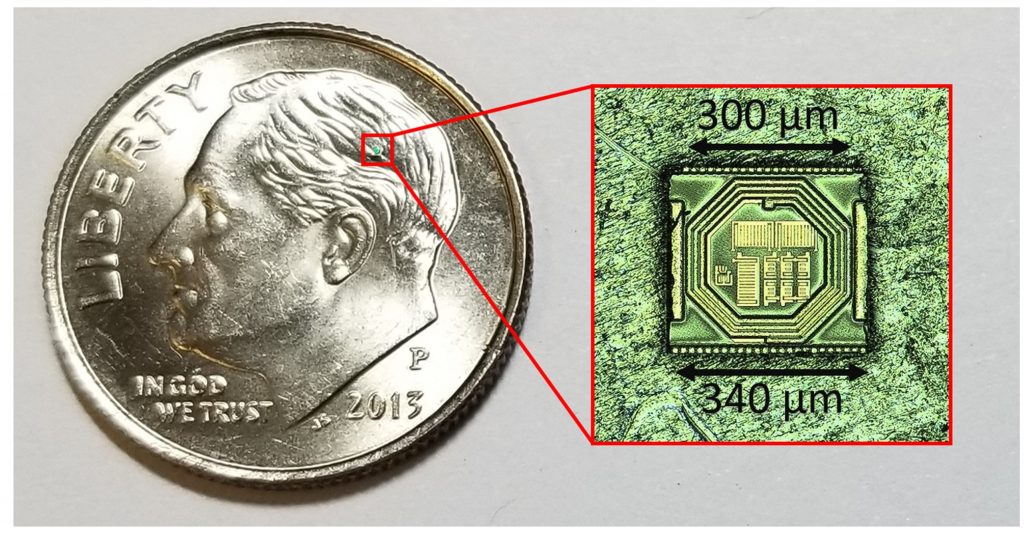
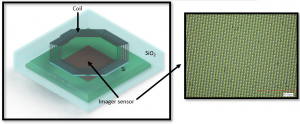
Wirelessly-powered neural interfaces are usually made of an assembly of multiple different components, such as an off-chip coil/crystal, an ASIC chip, electrodes, and surface mount capacitors. The conventional methods used to connect these components increase the volume of the implant and decrease reliability. Therefore, the bulky external parts and the interconnections significantly limit the extent of miniaturization of the packaged implant. To solve this issue, we have developed a novel process flow that incorporates all these separate parts into the ASIC chip.


On-going work:
- We plan on finding additional ways to exploit IC technology to avoid conventional bulky assembly methods. This allows us to miniaturize IMDs even further to make them injectable using minimally invasive surgical techniques.
- As conventional methods typically involve photolithography to fabricate microelectrode or expose the integrated electrodes, we will develop new process flows that rely on ink-jet printing to decrease the complexity and costs of current methods to encapsulate IMDs and integrate their electrodes.