Goal: Developing innovative circuit and system solutions for implantable devices
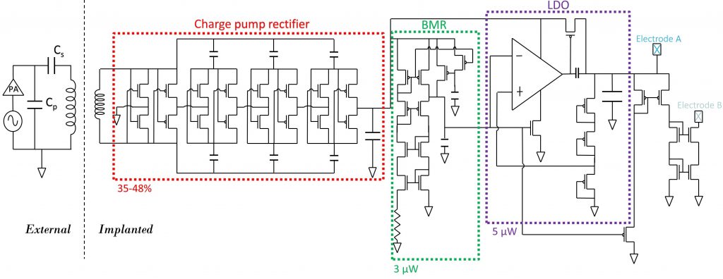
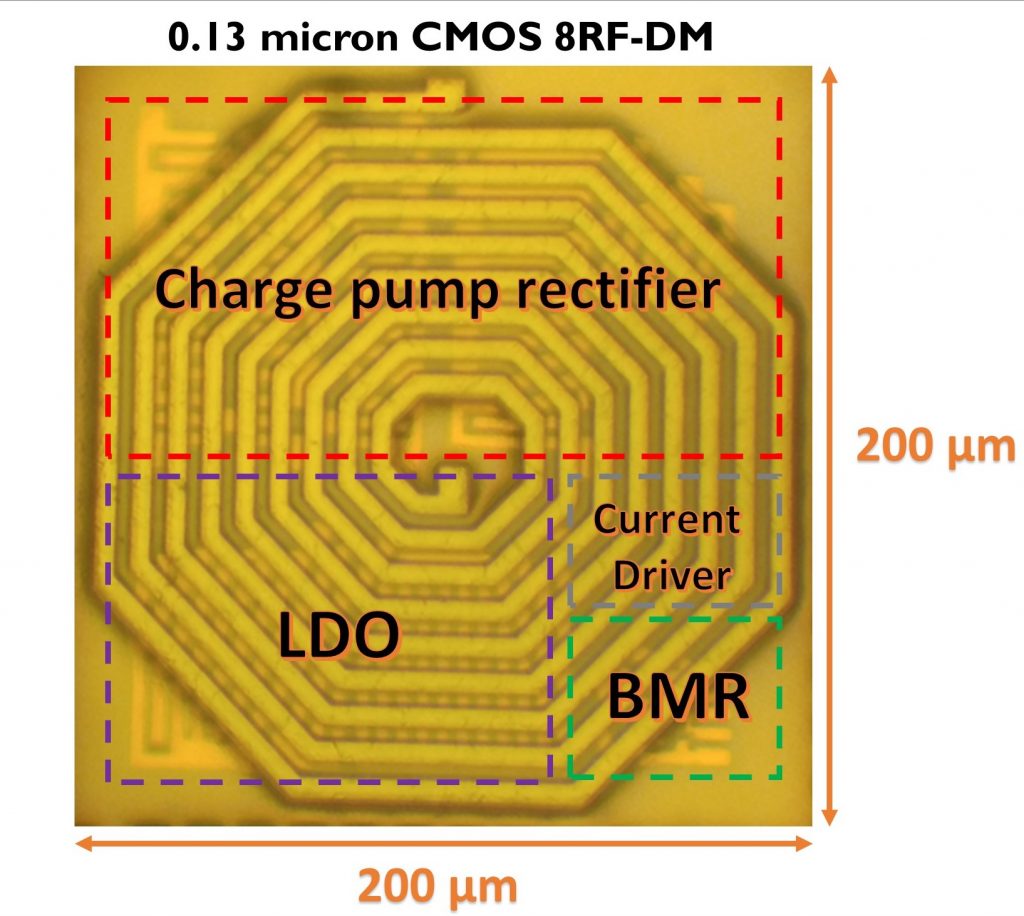
One of the key components of miniaturized wirelessly powered IMDs is the ASIC. There is a large need to decrease microdevices’ volume and power consumption, particularly those used to interface with neurons in the CNS. We have developed microdevices that can record neural activity and microdevices able to induce activity. We have fabricated various versions of recording and stimulating microdevices in 180, 130, and 32nm CMOS processes. On average they occupy less than 200µm × 200µm and consume less than 30μW.
On-going Work:
- We plan to further lower the area and power consumption of the microdevices by implementing novel circuit designs, using smaller fabrication nodes, and relying on silicon on insulator technology that is more ideal for RF circuits and inductive links. We are working on combining both recording and stimulation capabilities onto a standalone ASIC to target closed-loop neuromodulation applications. The uplink communication will be established by having the IMD communicate with the external system using backscatter modulation. We expect the new ASIC prototypes to measure less than 100µm × 200µm and consume less than 5 μW.
- We plan to develop novel energy harvesting ASICs for inductive wireless power transfer. The power management system will rely on an adaptive matching network to compensate for load, resonance frequency, and Tx-Rx distance/alignment/orientation variations.